
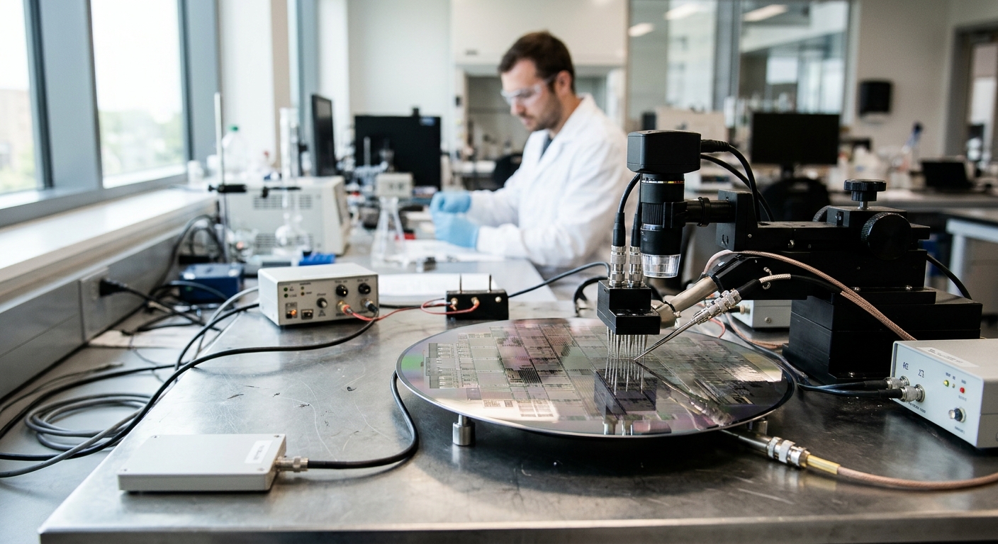
AI-generated illustration; not a photograph of the reported event.
- calendar_today October 30, 2026
Ohio State Hosts Ribbon-Cutting for Major Semiconductor Facility Expansion
The Ohio State University celebrated the opening of an expanded semiconductor research and prototyping facility on October 20, marking the completion of a project valued at over $20 million. The ribbon-cutting ceremony introduced new research and development infrastructure designed to accelerate the transition of semiconductor technologies from university research toward defense and commercial manufacturing. The upgrade also supports workforce development and hands-on student training.
Advancing Semiconductor Research and Industry Partnerships
The new capabilities are operated by the Institute for Materials and Manufacturing Research (IMR) and are part of the Microelectronics Innovation and Technology Cluster (MITEC). This initiative connects and enhances Ohio State’s existing resources for semiconductor processing, device prototyping, and testing. The expanded infrastructure aims to bolster both small and large industry partnerships and support technology development for national defense.
Support from the Midwest Microelectronics Consortium
MITEC will play a central role within the Midwest Microelectronics Consortium (MMEC), a regional innovation hub designated by the Department of War. MMEC’s CEO, Matt Casto, highlighted Ohio State's alignment with the consortium's mission to strengthen the United States’ microelectronics capabilities and supply chain. Casto remarked, "MITEC represents more than an investment in infrastructure; it brings together world-class expertise, advanced facilities and industry partnerships to accelerate the development and transition of critical semiconductor technologies."
Significant Investments Fuel Technology Development
The project is funded by approximately $16 million from MMEC and an additional $4.5 million through a collaborative investment from Ohio State and the Ohio Department of Higher Education. These investments have enabled the acquisition of advanced equipment and significant facility upgrades, enhancing Ohio State’s support for university researchers and private industry partners in developing, evaluating, and preparing cutting-edge semiconductor technologies for manufacturing.
Integrated Facilities for Flexible Prototyping
Led by Steven Ringel, Distinguished University Professor and senior associate vice president for research at Ohio State, MITEC incorporates resources from the Nanotech West Lab and the Semiconductor Epitaxy and Analysis Laboratory. This integration offers a flexible environment for collaborative technology development and rapid semiconductor prototyping.
Bridging the Gap Between Research and Commercial Manufacturing
MITEC supports semiconductor research and prototyping using wafer sizes and processes compatible with industrial manufacturing, allowing development and device testing at scales suited for commercial manufacturing. This capability shortens the time needed for new technologies to progress from academic laboratories to industry adoption and commercialization.
Focus on Workforce Development and Student Training
Workforce development and experiential learning are key components of the MITEC mission. MMEC-sponsored fellowships offer undergraduate and graduate students hands-on experience in cleanroom environments at Nanotech West Lab. Students engage with wide bandgap semiconductors for high-power and high-speed electronics, as well as narrow bandgap materials for infrared sensing applications. The training under experienced staff not only educates students but also accelerates the pace of technology development.
Positioning Ohio State as a Leader in Microelectronics Innovation
Ohio State’s enhanced infrastructure positions the university at the forefront of microelectronics innovation, strengthening its capacity to support device development and prototyping for both defense and commercial applications. This initiative demonstrates the institution's commitment to its land-grant mission of generating and sharing new knowledge, fostering economic growth, and building partnerships that benefit local and national technology ecosystems.
Related coverage
Source: news.osu.edu.